1. Background
The rapid development of advanced packaging and board-level packaging technologies is mainly due to the explosive growth in computing power demand, the inevitable choice in the post-Moore's Law era, and clear market growth expectations. In 2024, the global advanced packaging market reached $51.3 billion (accounting for nearly 50% of the overall packaging market), and is projected to grow to $91.1 billion by 2030, with a compound annual growth rate (CAGR) of approximately 10%. Board-level packaging (PLP), as an important direction within this market, has vast potential for substitution.
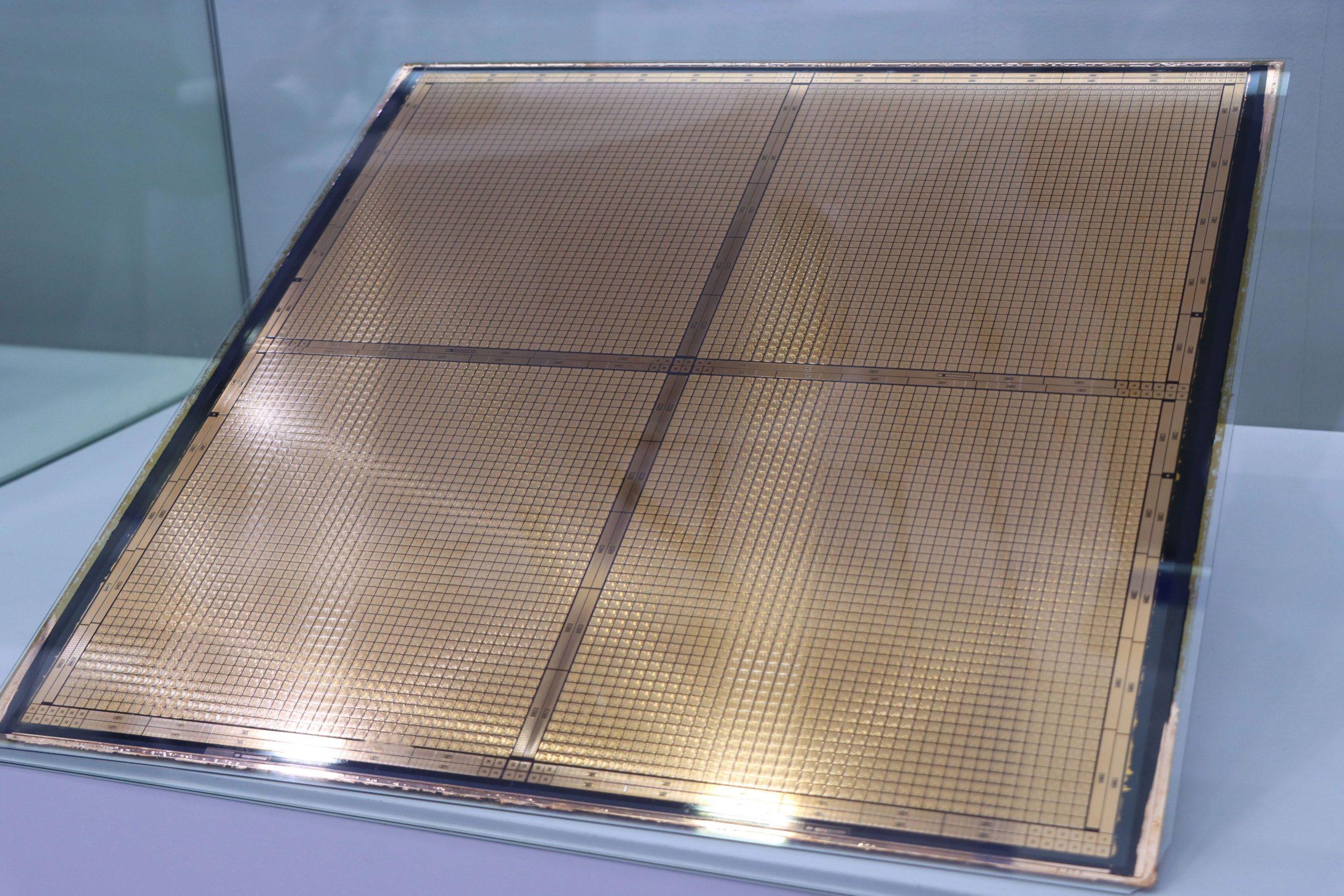
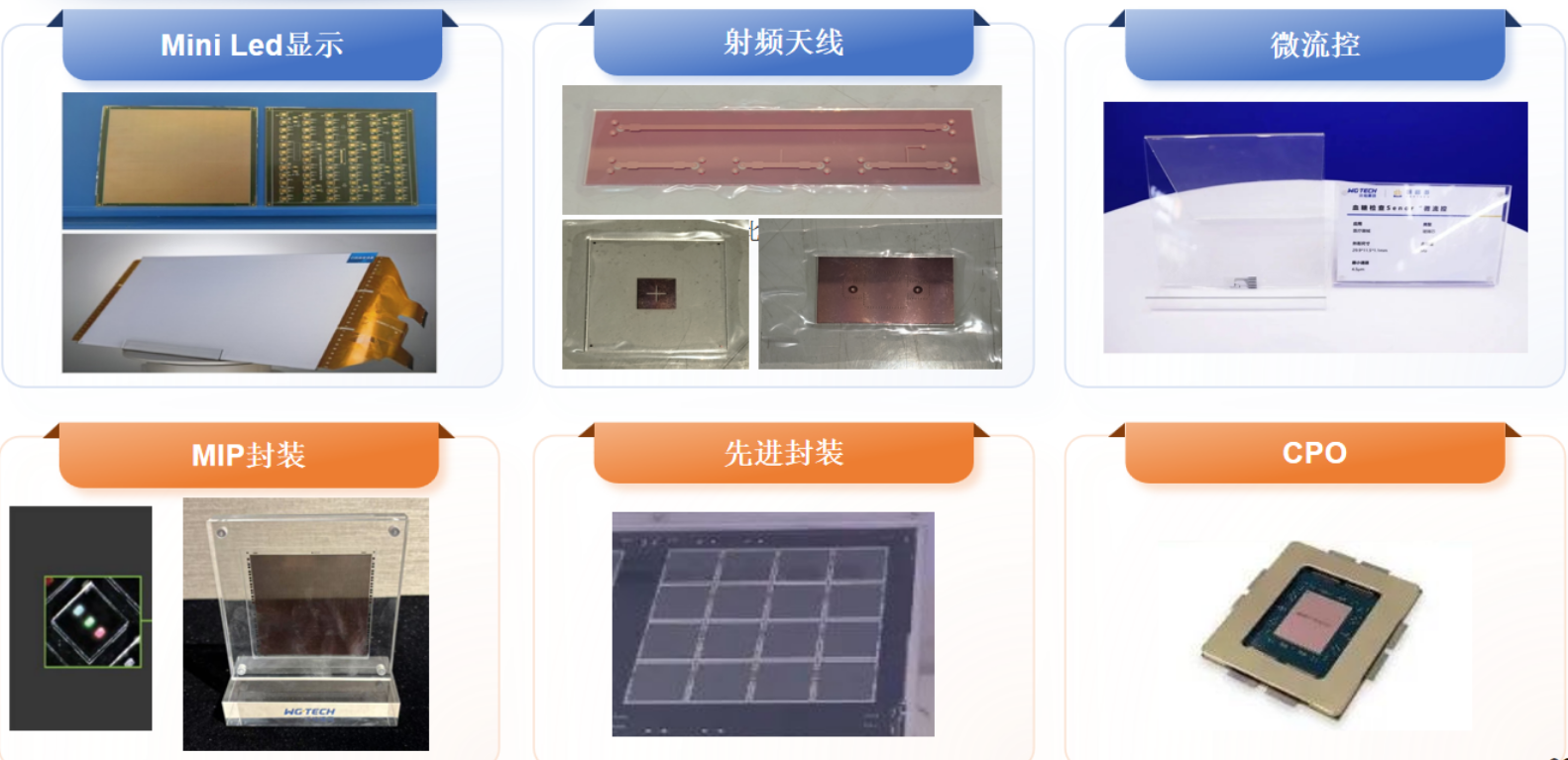
Photo taken at Yicheng Technology
Panel-level packaging (PLP) is an attractive branch of advanced packaging, its core value lying in its significant cost reduction potential, excellent electrothermal performance, and greater design flexibility: it facilitates heterogeneous integration, allowing chips from different process nodes and with different materials (such as CPUs, GPUs, and memory) to be integrated together to achieve better system-level performance.
High-end GPUs (such as NVIDIA and AMD series) and AI accelerator chips widely adopt 2.5D advanced packaging technologies such as TSMC's CoWoS. PLP is expected to provide more cost-effective solutions for these areas in the future. However, its development also faces some challenges, such as thermal stress management, TGV process complexity, and warpage issues with large panels.
Applications of Woger TGV in the semiconductor industry. (Image source: Woger Optoelectronics, Tongge Microelectronics)
However, with the collaboration of the industrial chain, technological innovation, the active deployment of various enterprises, and the acceleration of domestic substitution, the large-scale production of glass substrates may be promoted. It is expected that 2026 will become the "first year" of large-scale production of glass substrates, which will be applied first in high-end AI chips, data centers and other fields.
In order to continuously promote the development of the industry, promote upstream and downstream exchanges, and jointly explore market opportunities, Abang Semiconductor will hold the 3nd Glass Substrate TGV and Board-Level Packaging Industry Chain Summit Forum in Suzhou on March 19-20, 2026. We look forward to your participation and exchange.
Organizers:
Shenzhen Aibang Intelligent Manufacturing Information Co., Ltd.
Website: www.ab-sm.com
Time:March 19-20, 2026,Suzhou
2. Agenda
(Including but not limited to the following issues)
| NO. | topic | company |
| 1 | Glass core substrate: a new generation of advanced packaging technology | AKM Meadville Electronics (Xiamen) Co., Ltd. |
| 2 | Development and Prospect of Advanced Packaging Technology for Glass Substrates | Glassmicro (Chongqing) Semiconductor Tech. Co., Ltd. |
| 3 | All-glass multilayer interconnect substrate technology for advanced packaging of multi-core heterogeneous structures | Hubei TGVTECH Co., Ltd. |
| 4 | Application of Multiphysics Simulation Technology in Glass-Based Advanced Packaging | Hunan More Than Moore Advanced Semiconductor Co.,Ltd. |
| 5 | Development Trends of High-Density Glass Panel Packaging Technology | Chengdu ECHINT Technology Co., Ltd. |
| 6 | Breakthrough in TGV3.0 Through-Hole Structure Control and Metallization Synergistic Packaging | 3D CHIPS (GUANGDONG) TECHNOLOGY Co., Ltd. |
| 7 | Silicon-based optoelectronics fusion advanced packaging technology for high-computing applications | National Center for Advanced Packaging Co., Ltd. |
| 8 | Fundamental Problems and Limits in TGV Glass Through-Hole Laser Processing | Southern University of Science and Technology |
| 9 | Glass substrate optoelectronic bonding technology | Xiamen Sky Semiconductor Technology Co.Ltd. |
| 10 | EDA Accelerates the Design and Application of Glass-Based Devices | Xpeedic Co.Ltd. |
| 11 | Research on Key Technologies of High-Reliability 3D Integrated System (IS) and Advanced 3D IC Packaging | Rigger Micro Technologies Co.Ltd. |
| 12 | PVD system for 3D packaging | Arrayed Materials (China) Co., Ltd. |
| 13 | Transforming the Circle into the Square: Panel-Level Packaging (PLP) Enables the Future of Heterogeneous Integrated Chips | Manz China Suzhou Ltd. |
| 14 | Design Exploration of Glass-Based Chip Factory | China Electronics System Engineering Second Construction Co., Ltd. |
| 15 | Applications of magnetron sputtering deep hole coating in TGV field | Guangdong Huicheng Vacuum Technology Co., Ltd. |
| 16 | TGV PLP Via Filling Board-Level Electroplating Via Filling Solution
|
Kunshan Dongwei Technology Co., Ltd. |
| 17 | Laser-induced deep etching technology is not limited to TGV | LPKF Shanghai Co., Ltd. |
| 18 | Non-destructive testing of TGV laser-induced holes, etched holes, and metallization | Spirox Technology (Shanghai) Co., Ltd. |
| 19 | A significant milestone in the localization of advanced packaging and coating equipment. | Suzhou Precision System, Inc. |
| 20 | Key process development and industrialization of "Sputtering equipment for mass production of large-scale glass through-hole substrates" | Arison Surface Technology(Su zhou)Co.,Ltd |
| 21 | Applications of board-level fan-out packaging in power chips and modules | Shenzhen SiPTORY Technology Co., Ltd. |
| 22 | Next-generation electronic circuit and glass substrate TGV interconnect solution | Shenzhen Sai Mu Xi Jin Technology Co., Ltd. |
| 23 | Non-destructive testing of TGV laser-modified holes, etched holes, and metallized holes. | Currently soliciting |
| 24 | Enabling the Advanced Packaging Industry with HVM Solutions for Next-Generation Glass Core Substrates | SCHMID Group | SCHMID Technology (Guangdong) Co. Ltd. VicePresident Dr.Buchner Christian |
| 25 | Developing a wet chemical copper metallization process on glass substrates | Currently soliciting |
| 26 | Challenges of Metallized Interconnects in Heterogeneous Packaging
|
Currently soliciting |
| 27 | Discussion on advanced heat dissipation technology at the packaging level | Currently soliciting |
| 28 | High-efficiency RDL manufacturing technology: enabling panel-level packaging for various interconnect structures | Currently soliciting |
We are currently accepting submissions for more related topics. For speaking engagements and sponsorship inquiries, please contact Ms. Li: 18823755657 (same as WeChat).
3.Feedback Channel:
The final agenda and list of speakers will be updated in the near future and on the day of the conference. If you are interested in participating as a speaker or exhibitor at the 3nd TGV Forum, or if you are interested in opportunities for sponsorship, advertising, article submissions, conducting interviews, or if you have leading technology or product solutions, please contact Rongrong via email at lirongrong@aibang.com, Additional contact number: +8618823755657, or add Rongrong on WeChat: aibang360040.