
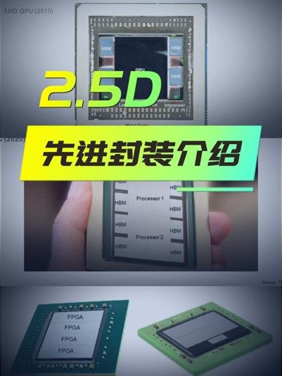
2.5D先进封装介绍(视频)
Hello everyone, welcome to Samsung. Today I'd like to talk about 2.5 d package technology, which is one of the hottest topics in package technology. First of all, what is 2.5 deep package technology?
大家好,欢迎来到我的节目。今天我们谈谈2.5D封装技术,这是封装技术中最热门的话题之一。首先,什么是2.5D封装技术?

扫描二维码,观看视频
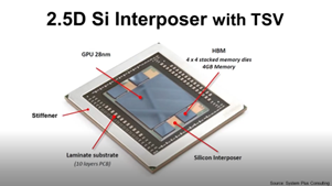
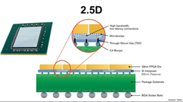
2.5 d looks like this. It is the packaging technology using silicone interpreter to connect dies on it. And silicon interposa has tsb through silicon via fabrical electrical interconnection. Then this silicon interpreter with dice are placed on package substrate to make package. Those dies can be multiple logic dies or logic die plus memory die. Prologic dies it can be f p g. Dies, g p u. Dies or network dies. This is the simplified structural 2.5 d to explain function of.
2.5D封装看起来像这样。它是使用具有硅通孔技术的interposer将不同的芯粒进行连接的技术。Interposer 嵌入在基板中,或者下面与基板相连,上面露出连接点,这样就可以将多个芯粒放置在连接点上 。这些芯粒的类型可以是逻辑芯片,高宽带存储的HBM,GPU等。 这是个简化版的示意图,可以看到最下层是基板,然后中间层是具有硅通孔技术的interposer,最上层是逻辑芯粒和存储芯粒。
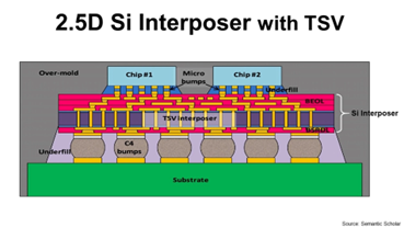
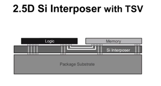
Type of silicone interpreter to connect logic die and memory die. For this case tap side of silicone temperature is also called as front side. More in detail, silicone interpreter has 3 part vertically. At top there is b e o l, back end of line layer which uses copper for electrical interconnection. If lining space of this carpet trace is fine less than 1μm it uses pol layer pie process but it can also use ideal for course copper trace at the middle there is tsp through silicon beer robotical electrical interconnection as its name implies tsp is a beer go through silicone supporter robotical electrical interconnection at the bottom there is r d l because it usually calls cafa trace bottom side of silicone interposter is also called as backside.
再看看更详细的示意图,Interposer 大致分为三层,最上面的一层是BEOL层,中间是TSV 硅通孔层,最下面是BSRDL层。BEOL层也叫back end of line layer, 利用铜层进行连接。TSV 硅通孔层用于连接上下两层。BSRDL 层也叫back side 重布线层。Interposer起到类似桥梁的作用将基板与芯粒连接起来。

Let's compare 2 d and 3 d to understand what is 2.5 d to the package. Is conventional package structure with dye with wire wounding or primitive. It also can be more than 2 dice side by side or stack dice, but they are not connected each other directly. How about 3 d? As you can see in the picture, chip a is connected with chip b with micro bump and chip b is connected with packet substrate at the bottom. Through tsb. We call this structure as ready.
让我们对比一下2 D和3D封装的区别,这样可以更好的了解什么是2.5D。2D 是传统的封装形式,芯粒通过wire bounding 的线连接与基板相连,或者通过基板上的C4与芯粒上的BUMP进行连接。2D也可以同时放置多个芯粒,但这些芯片互相不会堆叠在一起,互相通信通过基板相连。而3D是什么样的呢?如图所示,芯粒A与芯粒B通过微凸点连接,芯粒B 通过TSV与底部的基板连接。

What is the difference between 2.5 d and 3 d? Dies in 2.5 z package are electrically connected through silicone interposa, but Dyson 3 d is electrically connected directly. 2.5 d has tsb in silicone interposa, but 3 d has tsb in dice or one of dice cheaply for this case. This is an example of 2.5 d for fpgas.
2.5D和3D进一步还有什么具体的区别呢?如示意图所示,2.5D封装的芯片通过interposer将两个芯粒进行连接。而3D封装则是两个芯粒堆叠并直接相连,其中一个芯粒直接与基板连接。 3D封装中的一个芯粒具有TSV 硅通孔结构。
Jailing's apj company breaks one big apga die into 4 pieces, then put on silicone interpreter to connect each other. Because if you make vapors with big fpz dyes, die yield will be low, but if he split into smaller dyes die yield will be better.
这是一个2.5D FPBGA的芯片,整个芯片由4个芯粒组合而成,中间为interposer层将芯粒与基板连接。为什么要不直接组成一个芯粒呢?这主要是成本的考虑。小的芯粒良率更高,成本更低。
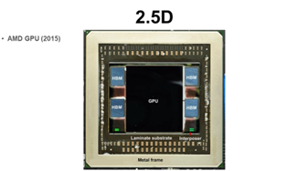

In 2012, jailings announced industry first 2.5, the package with silicone interpreter for their apga product. Another example is per GPU from AMD. In 2015 AMD combined GPU and hpm. Compare with previous solution GPU plus gddr gripping memory. Its size was much smaller with better performance. This is cross section of GPU plus hpm combination. Hpm by itself also have multiple DM dye stacks and tsp inside of DM dye. Sem's image of actual product looks like this. Nbdia also had GPU plus HBM combination in 2016.
2012年,赛灵思发布了业界第一款2.5D 封装的FPGA 产品。另外一个产品是AMD 2015年发布的GPU。AMD这款GPU结合了GPU和高宽带存储的HBM 。与以前的解决方案相比,这款GPU尺寸更小,性能更好。这是GPU加HBM的横截面示意图。HBM本身也有多个芯粒堆叠。实际产品的SEM图看起来像这样。英伟达在2016那年也有类似的GPU加HBM的组合产品。

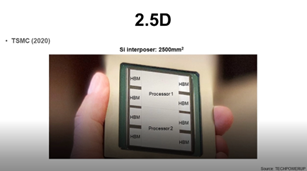
Stiepener at peripuri is to minimize package warpiece. Another example is broadcom network switch in 2018. It integrated network switch die and hpm memory on silicon interposa. Typically silicone interpreter is made by a foundry and major players are tsmc, umc, global founders, etc. In 2020 tsmc announced their latest 2.5. This solution with huge silicone temperature. It has 2 processor dies at the center and 8 hpm modules around. It uses 2000500mm² size silicone interpreter and tsmc plan to start mass production from 2023 this is a brief introduction to 2.5 deep package technology with silicone interposa I hope this can help you to understand basic two point five the package technology have a nice day and see you again soon bye bye.
Stiffener 是外面的加强框架,主要是来减少基板翘曲变形。另一个例子是2018年Broadcom的产品。它将网络交换机芯粒和HBM存储器芯粒通过interposer集成在基板上。通常2.5D封装由代工厂制造,当前的主要参与者有台积电、联电、格芯等。2020年台积电宣布了他们最新的2.5D封装。这种产品具有2个处理器芯粒,周围有8个HBM芯粒。它使用的interposer 有2500mm²。希望这个视频可以帮助你了解2.5D封装技术,再见。

扫描二维码,观看视频