
1. Conference Background
As Moore's Law approaches its physical limits, advanced packaging has become the critical path to sustaining semiconductor performance gains. TGV (Through Glass Via) technology—leveraging glass's excellent electrical insulation, low dielectric loss, tunable CTE, and the ready availability of large-format ultra-thin glass—is accelerating from the lab to commercialization. 2026 is widely regarded by the industry as the inaugural year of glass substrate commercialization. According to Omdia, the global packaged glass substrate market is projected to exceed USD 32 billion by 2030; CITIC Securities estimates glass-based carriers will begin small-batch shipments from 2027, with a potential market of over RMB 70 billion by 2030. Academician Peng Shou of the Chinese Academy of Engineering predicts this "super glass" could grow into a trillion-RMB market during the late 15th Five-Year Plan period.
On the process front, core links continue to break through. LPKF has completed TGV formation validation on glass exceeding 2 mm in thickness; its LIDE technology achieves a minimum aperture of 5 μm, an aspect ratio of 1:50, and has raised its addressable advanced-packaging TGV market forecast for 2030 to EUR 1.7 billion. Iris Nano's large-format TGV glass substrate through-via metallization PVD nano-coating material received Jiangsu Province's "Three Firsts & Two News" certification, solving uniform sidewall metallization in high-aspect-ratio vias. On the equipment side, Hymson now offers semi-turnkey delivery covering proprietary ultrafast lasers, laser drilling, and wet etching, with via roundness above 98%; HGTECH's TGV equipment core components are 100% domestically sourced; DR Laser's TGV laser modification systems continue to secure orders, including turnkey-line wins.
On the industrialization front, the global race is on and mass-production timelines are crystallizing. Intel has showcased EMIB plus glass-core substrate samples, targeting scaled ramp in 2027. TSMC is focused on CoPoS, with pilot production expected in 2027 and volume production in 2H 2028. Samsung Electro-Mechanics and Sumitomo Chemical formed the GlaSSEM joint venture, but reliability certification delays have pushed mass production past 2028. LG Innotek aims for glass substrate volume production in 2028. Domestically, BOE's glass-based packaging carrier pilot line has achieved full automation and sent samples to leading AI chip customers. WG Tech runs TGV capacity at 10,000 panels per month, with further expansion slated for 2027. Lens Technology signed an MoU with Intel to build a 30,000 m² dedicated TGV facility; its proprietary process delivers zero-ppm non-conductive rate across millions of vias. Linuo Pharmaceutical Packaging launched the LN33 glass substrate blank, with 150×150 mm samples passing TSMC performance tests. The full chain—from glass blank, equipment, and materials to TGV processing—is gradually taking shape.
On the application front, TGV is rapidly extending from semiconductor packaging into optical communications, optical interconnects, life sciences, and scientific consumables. At CIOE 2026, LX Tech, Semmar Electronics, and HGTECH showcased CPO optical interconnect solutions. Sandianji exhibited 310×310 mm panel-level interposers and 510×515 mm panel-level glass cores, while shipping volume glass-based micro-grid support films. AUO and Corning jointly presented a 510×515 mm glass core substrate and are investing NTD 8.641 billion in a pilot line. WG Tech and Avatarget Bio jointly launched the world's first glass-based organ-on-a-chip system. Industrial capital is accelerating entry: OFILM acquired a controlling stake in Zhongke Daojing; Rainbow Displays spun up Rainbow Semiconductor; panel makers BOE, TCL CSOT, and Tianma are all crossing over; WG Tech initiated the China Glass Circuit Board Industry Alliance.
Despite the broad outlook, TGV mass production still faces core bottlenecks. Current glass substrate yield sits around 70 percent—20 to 30 percentage points below ABF substrates. The pain points concentrate on three links: TGV drilling, multi-layer routing, and AOI inspection. Samsung's volume timeline has slipped at least three times, underscoring persistent challenges in brittle-glass handling, micro-via plating, and large-format warpage control. LPKF's CEO noted that the TGV process itself is no longer the bottleneck—true yield loss occurs in downstream copper filling and metallization. CICC judges that glass substrates are at the 0-to-1 stage, with 2027–2028 as the critical window for small-batch commercialization. The industry has moved from technology validation into pilot-line verification and capacity build-out; preliminary volume production is expected to land in 2027–2028.
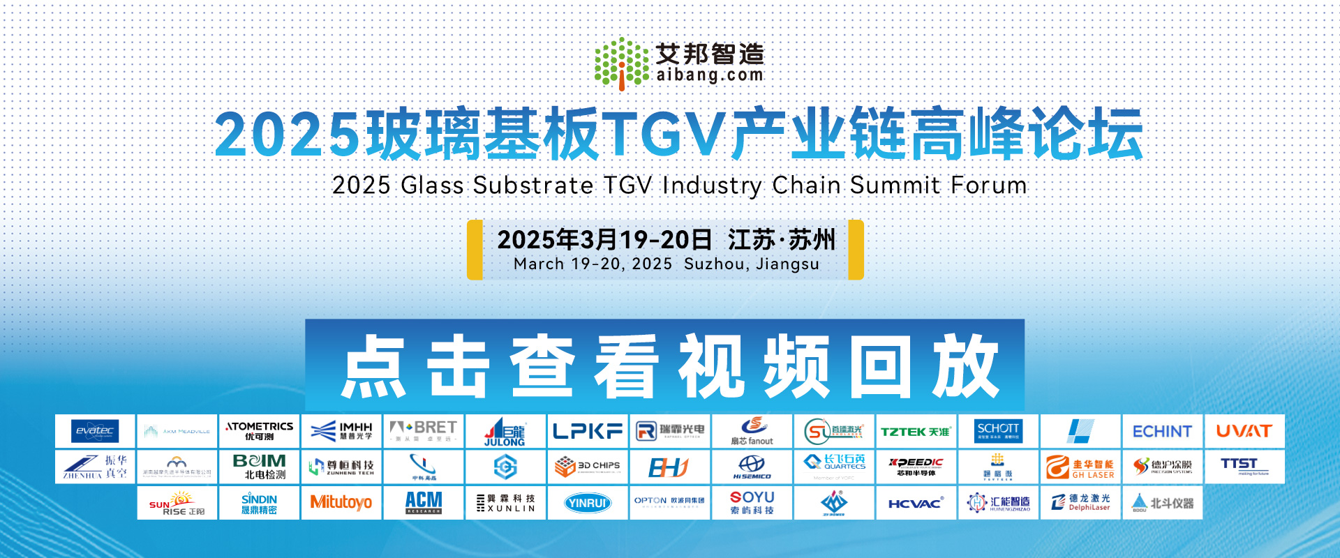
To that end, Aibang Semiconductor will host the 5th Glass Substrate TGV & Advanced Packaging Industry Chain Summit Forum on March 18–19, 2027 in Suzhou, Jiangsu, aiming to build an open, professional exchange platform. It will convene experts and enterprise representatives across materials, equipment, manufacturing, packaging, and end applications to discuss the latest TGV progress, process hurdles, market trends, and supply-chain collaboration paths. Through deep technical sharing and industry dialogue, we hope to tighten upstream-downstream cooperation and accelerate the maturation and commercial deployment of TGV technology.
II. Preliminary Topics
(agenda items to follow)
| No. | Topic |
| 1 | Review of the Inaugural Year of Glass Substrate Commercialization and Outlook on Mass-Production Milestones |
| 2 | Latest Breakthroughs in Thick-Glass TGV Formation and the Path to Industrialization |
| 3 | Process Challenges and Solutions for High-Aspect-Ratio Via Metallization: Seed Layer Deposition |
| 4 | Full-Process Yield Management for Glass Substrate Ramp-Up |
| 5 | End-to-End Inspection and Metrology Solutions for Glass Substrates |
| 6 | Glass Substrates in CPO Optical Interconnects and Progress in High-Speed Optical Engines |
| 7 | Glass-Based Organ-on-a-Chip: TGV's Cross-Over Exploration in Life Sciences |
| 8 | Domestic Glass Blank Technology and Matching Advanced Packaging Material Requirements |
| 9 | Latest Progress in Laser Drilling Equipment for Glass Substrates |
| 10 | Additive TGV Circuit Boards via Copper Paste: A Low-Cost Metallization Route |
| 11 | Warpage Control and CTE Matching Strategies for Large-Format Glass Substrates |
| 12 | Cleaning Technology in Hybrid Bonding for Advanced Packaging and Glass Substrate Applications |
| 13 | Glass Optical Waveguide Technology: Ion-Exchange Solutions for Optical Interconnects |
| 14 | High-Energy Pulsed Power Supplies for Deep-Via Magnetron Sputtering Seed Layer Deposition |
| 15 | Domestic Substitution of Key Glass Substrate Materials: CMP Pads, Plating Chemistry, and Photoresists |
| 16 | Mask Technology for TGV Glass Substrates: Development and Commercialization |
| 17 | Glass Core Substrates vs. Glass Interposers: Route Comparison and Industrialization Choices |
| 18 | 2.5D/3D Integration of Glass Substrates in AI Compute Chip Packaging |
| 19 | Ecosystem Building and Cross-Stream Collaborative Innovation for Glass Circuit Boards |
| 20 | Metallization Equipment for Glass Substrates: PVD, Electroplating, and Copper Filling |
| 21 | Bonding and Debonding Equipment for Ultra-Thin Glass Processing |
| 22 | Mass-Production Practices of Glass Substrates in Mini/MicroLED Displays |
| 23 | TGV-Integrated Passive Devices for RF Front-End Modules |
| 24 | Reliability Analysis and Failure Mechanism Studies of Glass Substrates |
| 25 | Thermal Processing Equipment for Glass Substrates: Annealing, Curing, and Stress Control |
| 26 | Coater-Developer and Lithography Equipment for RDL Patterning on Glass Substrates |
III. Feedback Channel
The final agenda and speaker list will be updated progressively and confirmed ahead of the event. If you are interested in participating as a speaker or exhibitor at the 5th TGV Forum, or wish to explore sponsorship, advertising, article submissions, media interviews, or technology and product showcase opportunities, please contact Rongrong:
- Email: lirongrong@aibang.com
- Phone / WhatsApp: +86 188 2375 5657
- WeChat (search by ID): aibang360040