
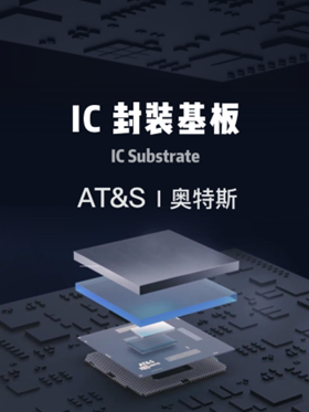
AT&S Explainer Movie - IC Substrate

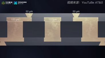
IC substrates provide powerful connections between the nanoworld of silicon DIEs and the micro world of PCBs. They are composed of several layers and a supporting core in their middle.The IC substrates contain drill holes and conductor paths that exceed the density of conventional PCBs by far. AT&S offers up to 8 laser drilled holes per square millimeter,
with diameters as low as 50μm we achieve a remarkable line spacing of 9 to 12 microns for the conductor tracks which has become standard for all AT&S IC substrate products
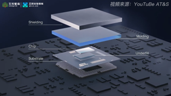
the next generation for further miniaturization is already in the research and development stage on the silicon DIEs interface side the IC substrate houses an ultra thin interconnection pattern in the form of a 100 micron solder mask grid, this complemented by a number of micro balls, makes the IC substrate ready for a smooth assembly of the silicon die. On the flip side, AT&S assembles SMT parts which finalize the IC substrate. Combined with the silicon die molding and shielding, the package is ready to deliver uncompromised performance.
IC基板在晶粒的纳米世界和PCB的微米世界之间提供了强大的联系。它们通常由多层组成,中间是支撑层。IC基板包含通孔和导电路径,其密度远远超过传统PCB。AT&S提供的基板激光通孔密度高达8个每平方毫米,直径低至50μm,我们甚至实现了9至12微米的极小线距,这已成为所有AT&S IC基板产品的标准。而针对下一代超薄及小型化产品及芯片的基板研究也处于开发阶段,其中包括CPU阻焊层网格为100微米的通过微焊锡球直接连接的产品。这些都为IC基板与芯粒更好的连接做好了准备。另一方面, AT&S还贴装SMT部件,最终完成IC基板成品。结合芯粒塑封及保护盖贴合,可以使封装的产品达到无与伦比的性能。
IC substrates by at AT&S for cloud, edge computing, data centers and server farms and for connectivity and user devices. Ats a reliable partner for complex semiconductor packages, making the future interconnected with IC substrates by AT&S.
IC基板用于云计算,边缘计算,数据中心和服务器场以及连接类个人设备。AT&S是先进半导体封装的可靠合作伙伴。 AT&S使未来与IC基板互连。
成员: 5306人, 热度: 153517
陶瓷 天线 通讯 终端 汽车配件 滤波器 电子陶瓷 LTCC MLCC HTCC DBC AMB DPC 厚膜基板 氧化铝粉体 氮化铝粉体 氮化硅粉体 碳化硅粉体 氧化铍粉体 粉体 生瓷带 陶瓷基板 氧化铝基板 切割机 线路板 铜材 氮化铝基板 氧化铍基板 碳化硅基板 氮化硅基板 玻璃粉 集成电路 镀膜设备 靶材 电子元件 封装 传感器 导电材料 电子浆料 划片机 稀土氧化物 耐火材料 电感 电容 电镀 电镀设备 电镀加工 代工 等离子设备 贴片 耗材 网版 自动化 烧结炉 流延机 磨抛设备 曝光显影 砂磨机 打孔机 激光设备 印刷机 包装机 叠层机 检测设备 设备配件 添加剂 薄膜 材料 粘合剂 高校研究所 清洗 二氧化钛 贸易 设备 代理 其他 LED